Creating critical high performance parts made from high performance polymers
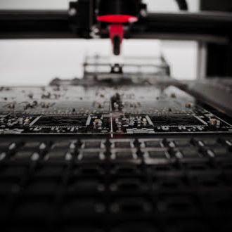
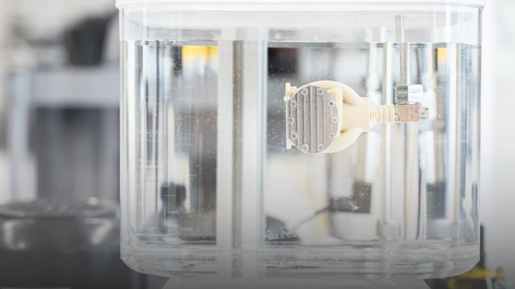
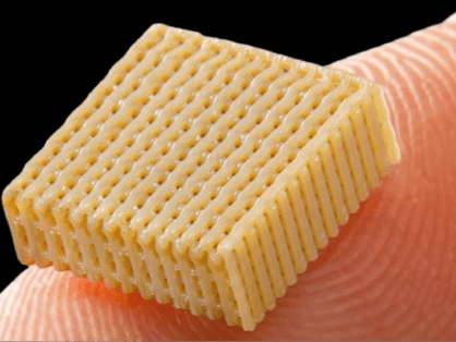
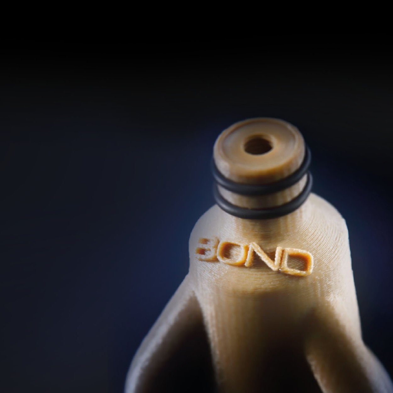
Creating critical high performance functional parts with additive manufacturing technology is a fast growing market but still limited by low strength in z-direction and voids. Bond3D as a pioneer in this market, has managed to maximize the possibilities of 3D printing with PEEK and optimize the process with a complete end-to-end solution by combining technology, material, and a skilled and dedicated team of specialists. High performance polymers which are printed with the Bond3D technology leads to functional products retaining its native material properties. The Bond3D technology is capable of printing PEEK in a voidless way, which allows for leak tight applications such as fluid and gas manifolds.
How we adapted our technology to print high performance polymers
At Bond3D, we decided to follow the reverse strategy and adapt the process to the material, to preserve its favorable properties in printed products. In principle this could be any polymeric material, but we put the focus on high-performance polymers such as PEEK. Our ambition was to develop a printer that produces functional end parts, not just prototypes, with properties that approach bulk values, concerning yield strength, leak tightness and chemical resistance.
- Unique patented High Performance Polymer printing technology e.g. The Bond3D technology)
- Adapt process to material to retain virgin material properties
- Printing certified and already approved high performance polymers
- Holistic approach, full system (hardware, system en software) in house developed
- Production & development in house
- Service provider
What are high performance polymers?
High-performance polymers such as aromatic polyimides, fluoropolymers, liquid crystalline polymers, polyaryletherketones, and sulfone polymers are widely used in automotive, aerospace, electric and electronic, industrial and medical applications that involve high temperature and extreme environment.
Even though they have a higher price compared to engineering plastics, they are chosen when their special features compensate for their cost. They are replacing conventional materials used in aerospace and automotive applications such as ceramics and metals mainly due to their lightness, high heat and oxidative resistance, chemical inertness, high dimensional stability and ability to maintain mechanical and physical properties over a wide temperature range. In addition, these plastics can be easily molded complex geometries components, offering design flexibility to satisfy continuous demand for component miniaturization, functional integration, safety and esthetic features that lead to their use in the automotive and electric and electronic application. Continuous research and development on these plastics aim to reduce overall manufacturing cost and widen their range of applications.
What is the difference between high-performance polymers and plastics?
There are many names for the term high-performance plastics, such as: high temperature plastics, high performance polymers, high performance thermoplastics or high tech plastics. The term “polymers” is often used instead of “plastics” when referring to a high performance plastic. Performance plastics are often achieved by the addition of stabilizers and reinforcing materials such as glass and carbon fibers to increase the degree of polymerization.
Properties of high performance polymers
PEEK does not offer merely two or three properties that mark it as the polymer of choice when high performance is required; it has a whole variety of them.
Chemically unreactive
PEEK is able to resist the damage that can be inflicted in chemically aggressive operational environments, such as downhole in wells the oil & gas industry, in gears in machinery & automotive applications. It can resist jet fuel, hydraulic fluids, de-icers and insecticides used in the aerospace industry. This holds true over wide ranges of pressure, temperature and time.
High heat resistance
Tests have shown that VICTREX PEEK polymer has a continuous use temperature of 260°C (500°F). This can make it suitable for use in a wide range of thermally aggressive environments, such as those found in the process industries, in the oil and gas sector and inside the engines and transmissions of millions of vehicles. PEEK is able to tolerate friction and resist wear in dynamic applications like thrust washers and seal rings.
Difficult to ignite or burn
PEEK has excellent flammability performance and it resists combustion up to almost 600°C. When it can be made to burn at very high temperatures, it will not support combustion and it emits little smoke. This is one reason why PEEK is widely used in commercial aircraft.
Mechanically strong
PEEK demonstrates excellent strength and stiffness over a wide temperature range. PEEK-based carbon fibre composites have specific strength many times that of metals and alloys. “Creep” refers to a material becoming permanently deformed over an extended period of time when under constant applied stress. “Fatigue” refers to the brittle failure of a material under a repeated cyclic loading. PEEK has both high creep and fatigue resistance thanks to its semi-crystalline structure and has been shown to be more durable than many other polymers and some metals over a long and useful lifetime.
Re-processable and recyclable
The PEEK molecule is very stable, so the polymer can be re-melted and reprocessed again and again with minimal change to its properties. This helps its environmental footprint and can ensure that waste material from manufacturing processes can be re-used economically.
Advantages of high performance thermoplastics
There are many names for the term high-performance plastics, such as: high temperature plastics, high performance polymers, high performance thermoplastics or high tech plastics. The term “polymers” is often used instead of “plastics” when referring to a high performance plastic. Performance plastics are often achieved by the addition of stabilizers and reinforcing materials such as glass and carbon fibers to increase the degree of polymerization.
Ease of Processing
Compared to other materials such as metals or ceramics, thermoplastics are relatively easy to process. They can be injection molded, extruded, or thermoformed into complex shapes with relative ease. This opens up a wide range of design possibilities.
Production Efficiency
Thermoplastics, due to their ability to be repeatedly heated and cooled without significant degradation, can be remolded and reshaped without the need for additional raw materials. This means that waste from the production process can be recycled back into the production stream, improving overall efficiency and sustainability.
Design Flexibility
The production process for high performance thermoplastics allows for a high degree of design flexibility. Different additives can be mixed in to give the plastic specific properties, and the molding process allows for the creation of complex shapes and forms that would be difficult or impossible to achieve with other materials.
Lower Energy Consumption
The production process of high-performance thermoplastics can be more energy-efficient compared to metals. The lower melting points of thermoplastics mean that less energy is required in the heating and molding processes.
Rapid Production
High-speed injection molding processes allow for rapid production rates, which can reduce lead times and increase the speed at which products can be brought to market.
Lightweighting
In the production process, thermoplastics can be manipulated to have high strength-to-weight ratios. This property is beneficial in industries such as automotive and aerospace where weight reduction is a key factor in improving efficiency and performance.
An unique combination for high performance polymers
Victrex 450G PEEK is a high performance polymer certified for use in the medical, aerospace and food industry. Due to its excellent properties the material enables the development of light weight and strong products applicable in demanding environments.
Bond3D Technology
- Preservation of material properties
- Voidless printing
- Isotropic strength
- Ultra High vacuum applications
- Pressure tight
- Engineering services
+ Additive Manufacturing values (AM)
- Flexible design
- Design for 3D modelling
- Complex internal structures
- Cost saving
- Speed to market
- Capital efficiency
PEEK 450G
• Wear Property
• Easy Processing
• Mechanical Strengths (TS 98 MPa)
• Bio inert (also radiolucent for X-ray, CT or MRI)
• Electrical Property (Insulating or conductive)
• Extreme Temperature (-40°C to +250°C)
• Chemical Resistance (also sterilization by Gamma)
• High Purity