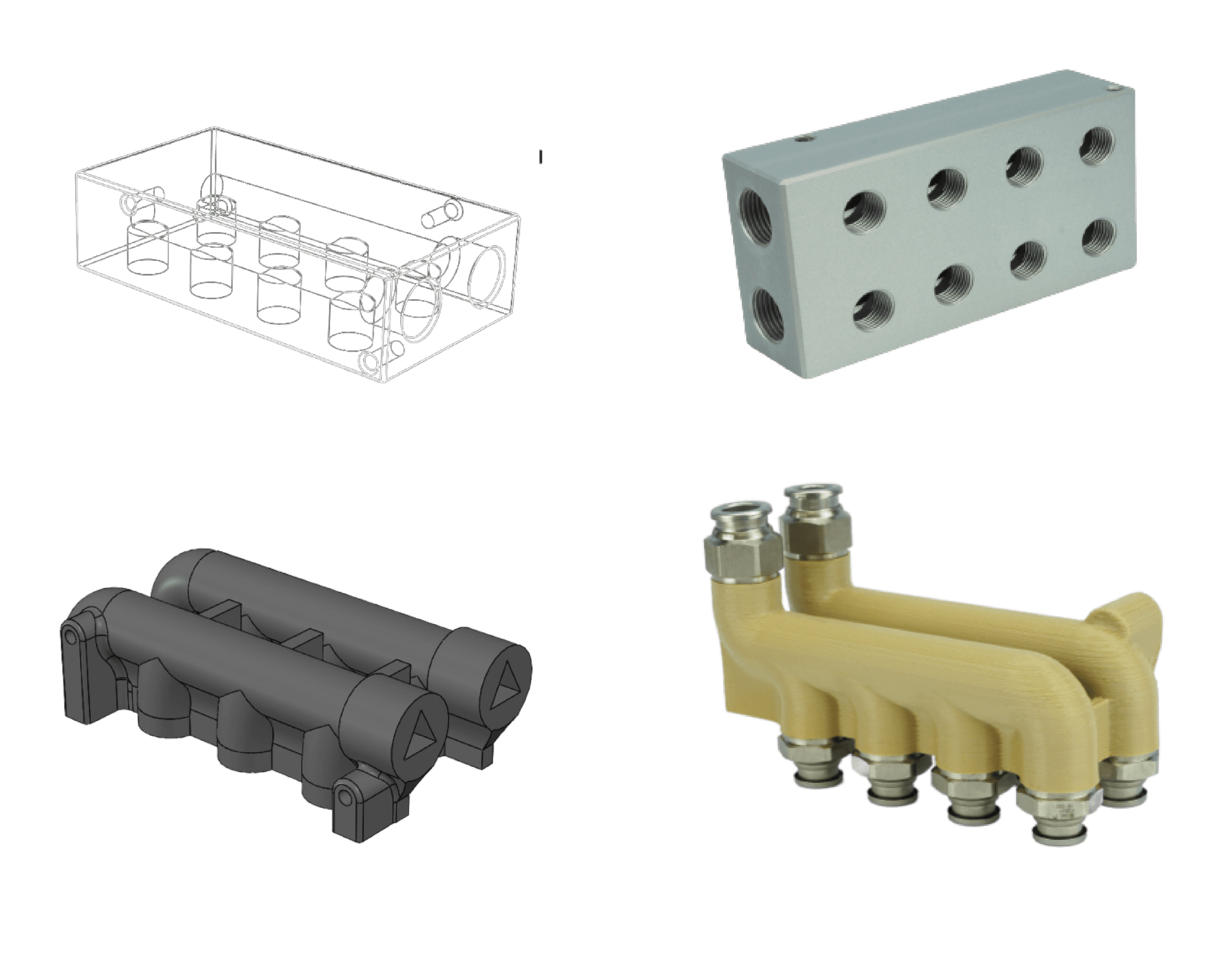
PEEK Cooling Manifold

Significant trends as mobile computing, internet-of-things and autonomous driving are pushing the electronics market, production of small volume high performance machine parts for manufacturing industry such as the semiconductor, to significant growth levels.
Industries providing the infrastructure for this demand are challenging ‘Moore’s law’ on a daily basis. Within this challenge performing materials such as PEEK are often recognized as a valuable material enabling new solutions.
Bond3D allows players in this field to work with 3D printed performing solutions of high performing plastics. Bond3D has experience in the electronic industry and understands the requirements of parts operating specifically in high vacuum environments.
PEEK’s excellent electrical properties make it an ideal insulator. With excellent thermal properties, PEEK polymer components can withstand high temperatures that conventional insulation cannot withstand. These benefits, along with long-term reliability, temperature, pressure, and frequency stability, make them suitable for use in subsea environmental control equipment or high-pressure pump terminal pins.
PEEK can maintain good electrical insulation even under harsh working conditions such as high temperature, high pressure and high humidity. Therefore, the application field of PEEK resin is gradually changing to the field of electronic and electrical appliances. PEEK resin has high purity and stable mechanical and chemical properties, which reduces contamination when processing silicon wafers.
PEEK resin does not deform over a wide temperature range and can be used to manufacture parts that can withstand the high temperatures of heat welding. Due to this property, PEEK resin is commonly used in the semiconductor industry to produce wafer carriers, electronic insulating sheets, various connecting devices, as well as wafer carrier insulating sheets, connectors, printed circuit boards, high temperature connectors, etc.
PEEK resins can also be used in µg/L ultrapure water handling and storage equipment such as pipes, valves, pumps and positioners. PEEK is already used in Japan and other countries in the manufacture of large scale integrated circuits. PEEK is used in plug-in connectors, high reliability connectors, cable connectors, junction boxes, distribution lines, plate cage coils, battery cases, IC packaging, the semiconductor industry, and other electronic and electrical applications in fittings and valves for ultrapure water systems. It can also be used in fields. Required in ultrapure industry and other components.
3D printing of high-performance polymers overcomes the restrictions of conventional manufacturing. It opens up a whole new world of design and production possibilities while optimizing your Cost of Goods.
Bond3D parts from PEEK are voidless and very well suited for complex structures that manage fluids and gas. Our printed parts can be pressurized to 100+ BAR.
Design and print strong functional parts with complex structures, like manifolds, which would be impossible to create with conventional methods.
PEEK parts can withstand temperatures from – 40 C up to + 250 C.
PEEK is up to three times lighter than titanium and 40% lighter than aluminum. Bond3D printing further enhances PEEK with weight-optimized designs.
Peek is very suited for cleanroom applications. Thanks to its low outgassing it is very useful in high vacuum environments.
PEEK printed with Bond3D technology has a high mechanical strength of 95MPa, which is close to the base-material properties.
PEEK is resistant to almost any chemical, making it the perfect material for demanding applications.
Simplify designs to reduce the failure rate and optimize up-time by reducing weak spots in designs.
Fast development, rapid prototyping, and short lead times ensure fast delivery.
Integrate multiple parts into one, i.e. manifolds with cable routing.
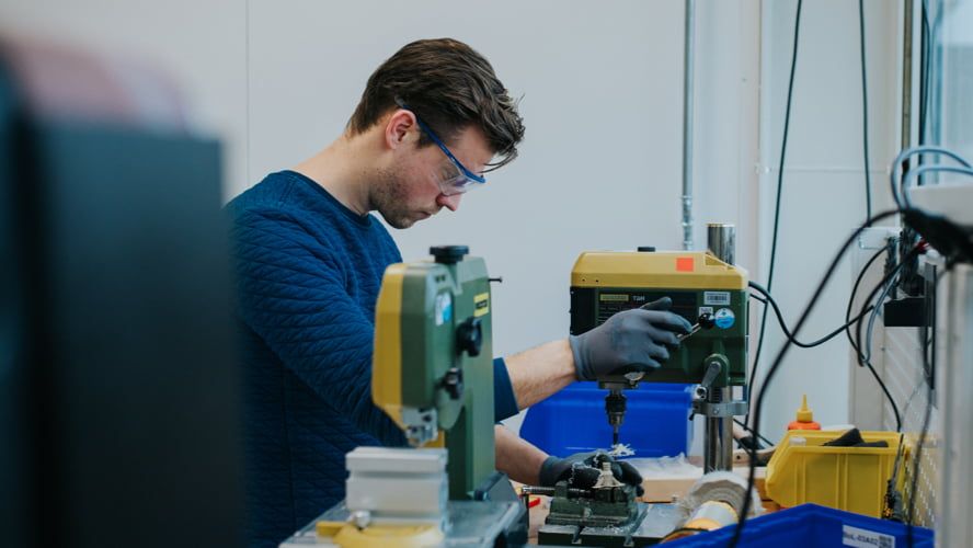
“Because of the leak-tight properties, 3D printed manifolds are an important part of our core business. It’s a critical application for the racing- and semiconductor industry where higher output or more efficient machines are essential” says Marc Kunst.
The application team at Bond3D can provide you with right analysis by checking how you can replace your conventional metal cooling manifolds with 3D Printed PEEK cooling manifolds.
We believe transforming manufacturing is a team effort. Let’s get in touch and discuss how we can help you take the next step.


